


The 74LS90 is a simple counter, i.e. it can count from 0 to 9 cyclically in its natural mode. It counts the input pulses and the output is received as a 4-bit binary number through pins QA, QB, QC and QD. The binary output is reset to 0000 at every tenth pulse and count starts from 0 again. A pulse is also generated (probably at pin 9) as it resets its output to 0000. The chip can count up to other maximum numbers and return to zero by changing the modes of 7490. These modes are set by changing the connection of reset pins R1 – R4. For example, if either R1 & R2 are high or R3 & R4 are ground, then it will reset QA, QB, QC and QD to 0. If resets R3 & R4 are high, then the count on QA, QB, QC and QD goes to 1001.
The other high counts can be generated by connecting two or more 7490 ICs. For example, if two 7490 are connected in a manner that input of one becomes the output of other, the second IC will receive a pulse on every tenth count and will reset at every hundredth count. Thus this system can count from 0 to 99 and give corresponding BCD outputs.
7490 has an inbuilt divide by two and divide by five counters which can be connected in different fashion by changing the connections. It can be used as a divide by 10 counter by connecting QA with (clock) input2, grounding all the reset pins, and giving pulse at (clock) input1. This enables the cascade connection of the inbuilt counters. It can also be used as a divide by 6 counter by connecting QA with input2, grounding R3 & R4, and giving pulse at input1.
By connecting QA with input1, 7490 can be used for BCD counting whereas by connecting QD with input2, it can be used for bi-quinary counting. Bi-quinary is a system for storing decimal digits in a four-bit binary number. The bi-quinary code was used in the abacus.
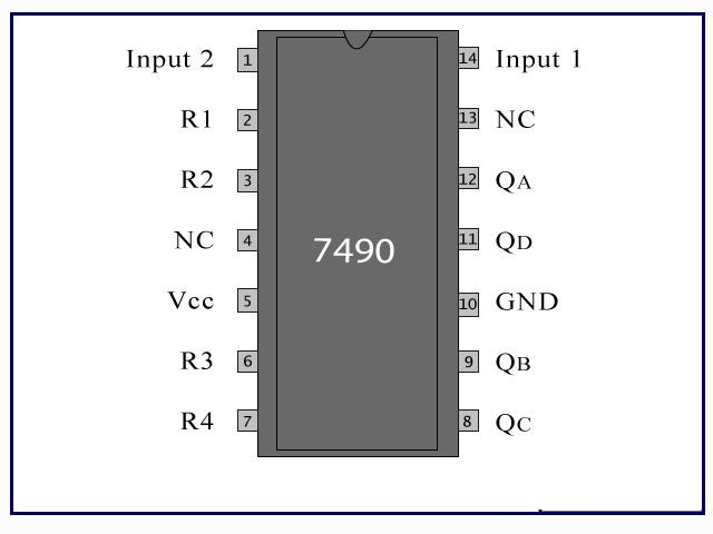
Pin Description:
| Pin No | Function | Name |
| 1 | Clock input 2 | Input2 |
| 2 | Reset1 | R1 |
| 3 | Reset2 | R2 |
| 4 | Not connected | NC |
| 5 | Supply voltage; 5V (4.75V – 5.25V) | Vcc |
| 6 | Reset3 | R3 |
| 7 | Reset4 | R4 |
| 8 | Output 3, BCD Output bit 2 | QC |
| 9 | Output 2, BCD Output bit 1 | QB |
| 10 | Ground (0V) | Ground |
| 11 | Output 4, BCD Output bit 3 | QD |
| 12 | Output 1, BCD Output bit 0 | QA |
| 13 | Not connected | NC |
| 14 | Clock input 1 | Input1 |


