

Many of us design PCB with the information available on internet but sometimes it becomes difficult to understand the terms used in PCB designing. In this article I have tried to explain the common terms which are used while designing PCBs. PCB stands for printed circuit board. Different types of PCB materials are available in markets. Most commonly used are FR-1, FR-2, CEM-3, CEM-1 (FR=Flame Retardant and CEM= Composite Epoxy Material).
Common terms used are as follows-
- Layers
Everything which you draw is on layer. Each layer has different physical properties. For example top layer is used to draw the component layout, bottom layer or inner layer are used for making connection between components and many more are also present.
- Footprint
Footprint is the collection of pads and outline which make an individual component. PCB design software comes with a library which contains footprints of different components but the number of [sam id=”5″ codes=”true”]footprints that are available is limited. As we know today technology is changing and size of components is reducing, so sometimes we have to make the footprint of the component.
- Solder mask
You all have seen the green, red, blue or shiny coating on the PCB. This coating is known as solder mask. Masking is done to avoid the solder which accidently drops on PCB and soldering of component also become easy. This also prevents the short circuit among close track. Being a beginner it may possible we use excess of solder while soldering which may short the tracks, if solder mask is there it can be easily removed without melting. This is a non conducting layer of a PCB.
- Silkscreen
Silkscreen is done to represent the name or value of components so that user can easily identify the component during soldering. This is a good practise while designing the PCB. Silk-screening can be done on both sides of PCB (on component side or on copper side). This can also be used to indicate the name of the company or manufacturer. This is a non conducting layer of a PCB.
- Jumper
Jumper wire forms electrical connections between two points on printed circuit board. Sometimes it happen while designing PCB that tracks may overlap each other as we make connections; in that case we used jumper wire.
- Pads
Pads are used to make connections between component and track with the help of solder.Pads are small surface of copper available on printed circuit board. They are basically used to solder the leads of the components on board to make the mechanical joint strong. Different kinds of pads are used for Surface mount component and through hole component as shape and size of both the components vary from one another.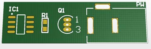
- Copper traces
You have seen that green, blue or red lines are used to connect pads and vias. They are known as copper traces. They provide electrical conduction between pads and vias or between two pads and vias. Width of track varies according to the current flow through them.
- Via
Suppose you are designing multilayer PCB and you want the connection between bottom layer and top layer then we use via. Via allows the current to pass through the board. This can be seen in the figure below. In this consider yellow colour pads as bottom layer and green colour pads as top layer so the yellow color circle shown are via.
Basically following colours are used to indicate the layers in multilayer PCB-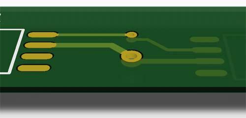
The PCB in figure shows a track that belongs to the top layer that goes through the board using a thru-hole via, and then continues a track that belongs to the bottom layer.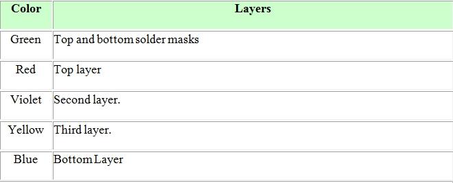
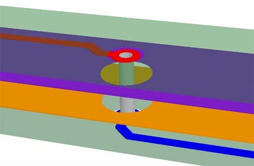
- Blind via
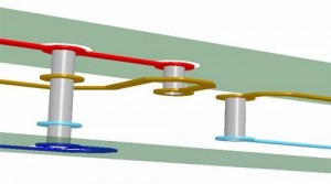
In more complex circuit generally in designing integrated circuits where more power planes (Gnd and Vcc) are used we prefer via. We used vias between top layer and second layer not in the bottom layer. These vias are called blind vias. Because it i easy to directly connect the power planes that are beneath the chips instead of routing long tracks. Blind vias are used when connection has to be made from external layer to internal layer with minimum vias height.
You can identify that the vias used are through hole or blind. Just put your PCB on source of light and see if light is coming from source through via. If you can see the light , then the via is through hole otherwise it a blind via. This technique is useful where you don’t have much space for placing the component and routing. If you use through hole via instead of blind then it would need some extra space by vias on both sides.
From the figure below you can see that one blind via is connect between top layer and inner layer(red colour and yellow colour) and another blind vai is connected between inner layer and bottom layer( blue and light blue). And in the similar figure where all three colour are present is a through hole via connecting top and bottom layer.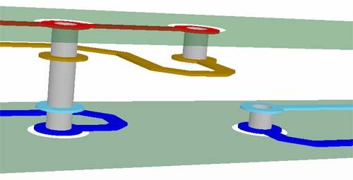
10.Buried Vias
Buried vias are similar to blind vias but they only make connection between the inner layers. From the figure you can see that yellow and light blue colours represent the buried vias. From figure below you can compare all three vias as follows-
- First one that is red yellow light blue and blue represent through hole via.
- Second one that is red and yellow represent blind via.
- Third one that is yellow and light blue represent buried via.
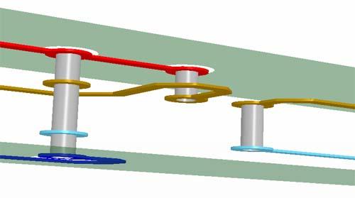
Main disadvantage of using buried via is it will increase the cost of PCB as compared to through hole via. But advantage of using buried vias is smaller size. So depending upon the requirement one can use the type suitable to it.
- Gerber
Gerber file is send by user to manufacture to make PCB. Gerber file is important because many PCB design software are available now a days and it is not necessary that software which you are using will be available at vendor side. Suppose I make my PCB on Eagle software and my PCB manufacturer does not have the same, at that time gerber file is useful. So now gerber file will help manufacture to know your project and manufacturer cannot make changes in gerber file. Gerber file contain information about drill size, where to make hole, how tracks are connected, naming of components etc.
- BOM
BOM represent bill of material. It gives you the list of component present on PCB. So that you can calculate the approximate cost and it becomes easy for you to order the components. With this you can cross check the components you forgot by mistake.


