

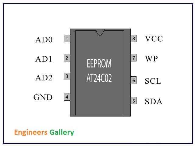
AT24C02 is an electrically erasable and programmable ROM. It has a 2Kbits of memory size arranged in 32 pages of 8 byte each. There are 256 (32 x 8) words each of one byte. The data is transferred and received serially through serial data (SDA) pin.
The SCL is clock input and is used to synchronize EEPROM with microcontroller for various operations. When data is to be read or write, first a start condition is created followed by device address, byte address and the data itself. Finally a stop condition is provided. The start condition occurs when SDA and SCL get high to low simultaneously. The stop condition is when SDA remains low while SCL goes from high to low. The data is read or written between the start and stop conditions on every transition of SCL from high to low. For more details on different operations and addressing, referinterfacing 24C02 with 8051.
A total of eight EEPROMs can be connected through a bus. There are three address pins in AT24C02 for selecting a particular chip. The device can be addressed serially by the software. It makes use of an internal register of the EEPROM whose 4 MSB bits are 1010, the next three are the EEPROM address bits and the LSB signifies whether data is to be read or written. This last bit is 1 for write and 0 for read operation.
For example, if in an EEPROM all address bits are grounded, then for write operation a hex value 0xA1 (1010 0001) will be sent. Here 000, in last bits, addresses the EEPROM and 1 in LSB indicates a write operation. Similarly for read operation the device address to be sent is 0xA0 (1010 0000).
Next, the byte or page address is sent followed by the data byte. This data byte is to be written on or read by the microcontroller.
Pin Description:
| Pin No | Function | Name |
| 1 | Address input pins; Provide addresses when more than one EEPROM is interfaced to a single microcontroller;Ground when only one EEPROM is used | AD0 |
| 2 | AD1 | |
| 3 | AD2 | |
| 4 | Ground (0V) | Ground |
| 5 | Bi-directional pin for serial data transfer | Serial Data |
| 6 | Provides clock signals | Serial Clock |
| 7 | Ground allows normal read/write functions;Vcc enables write protection | Write protect |
| 8 | Supply voltage; 5V (up to 5.5V) | Vcc |


