

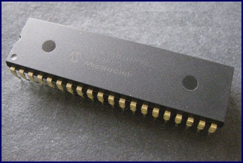
PIC18F4550 is an 8-bit microcontroller of PIC18 family. PIC18F family is based on 16-bit instruction set architecture. PIC18F4550 consists of 32 KB flash memory, 2 KB SRAM and 256 Bytes EEPROM.
This is a 40 pin PIC Microcontroller consisting of 5 I/O ports (PORTA, PORTB, PORTC, PORTD and PORTE). PORTB and PORTD have 8 pins to receive/transmit 8-bit I/O data. The remaining ports have different numbers of pins for I/O data communications.
PIC18F4550 can work on different internal and external clock sources. It can work on a varied range of frequency from 31 KHz to 48 MHz. PIC18F4550 has four in-built timers. There are various inbuilt peripherals like ADC, comparators etc in this controller.
PIC18F4550 is an advanced microcontroller which is equipped with enhanced communication protocols like EUSART, SPI, I2C, USB etc.
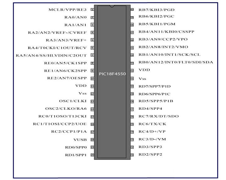
Pin Description:
| Pin No. | Name | Description | Alternate Function |
| 1 | MCLR/VPP/RE3 | Master clear | Vpp: programming voltage inputRE3: I/O pin of PORTE, PIN 3 |
| 2 | RA0/AN0 | PortA I/O Pins 1-6 | AN0: Analog input 0 |
| 3 | RA1/AN1 | AN1: Analog input 1 | |
| 4 | RA2/AN2/VREF-/CVREF | AN2: Analog input 2VREF-: A/D reference voltage (low) input.CVREF: Analog comparator reference output. | |
| 5 | RA3/AN3/VREF+ | AN3: Analog input3VREF+: A/D reference voltage (high) input | |
| 6 | RA4/T0CKI/C1OUT/RCV | T0CKI: Timer0 external clock input.C1OUT: Comparator 1 outputRCV:External USB transceiver RCV input. | |
| 7 | RA5/AN4/SS/HLVDIN/C2OUT | AN4: Analog input 4SS: SPI slave select inputHLDVIN: High/Low-Voltage Detect input.
C2OUT: Comparator 2 output. |
|
| 8 | RE0/AN5/CK1SPP | PortE I/O Pins 1-3 | AN5: Analog input 5CK1SPP: SPP clock 1 output. |
| 9 | RE1/AN6/CK2SPP | AN6: Analog input 6CK2SPP: SPP clock 2 output | |
| 10 | RE2/AN7/OESPP | AN6: Analog input 7OESPP : SPP Enabled output | |
| 11 | VDD | Positive supply | |
| 12 | Vss | Ground | |
| 13 | OSC1/CLKI | Oscillator pin 1 | CLKI: External clock source input |
| 14 | OSC2/CLKO/RA6 | PortE I/O Pin 7 | CLKO: External clock source outputOSC2: Oscillator pin 2 |
| 15 | RC0/T1OSO/T13CKI | PortC I/O Pins 1-3 | T1OSO :Timer1 oscillator outputT13CKI: Timer1/Timer3 external clock input. |
| 16 | RC1/T1OSI/CCP2/UOE | T1OSI: Timer1 oscillator outputCCP2:Capture 2 input/Compare 2 output/PWM2 outputUOE: External USB transceiver OE output | |
| 17 | RC2/CCP1/P1A | CCP1: Capture 1 input/Compare 1 output/PWM1 output.P1A :Enhanced CCP1 PWM output, channel A. | |
| 18 | VUSB | Internal USB 3.3V voltage regulator output, positive supply for the USB transceiver. | |
| 19 | RD0/SPP0 | PortD I/O Pins 1-4 | SPP0-SPP4Streaming Parallel Port data |
| 20 | RD1/SPP1 | ||
| 21 | RD2/SPP2 | ||
| 22 | RD3/SPP3 | ||
| 23 | RC3/D-/VM | PortC I/O Pins 4-5 | D-: USB differential minus line (input/output)VM: External USB transceiver VM input. |
| 24 | RC4/D+/VP | D+: USB differential plus line (input/output).VP: External USB transceiver VP input. | |
| 25 | RC6/TX/CK | PortC I/O Pins 7-8 | TX: EUSART asynchronous transmit.CK: EUSART synchronous clock (see RX/DT). |
| 26 | RC7/RX/DT/SDO | RX: EUSART asynchronous receive.DT: EUSART synchronous data (see TX/CK).SDO: SPI data out. | |
| 27 | RD4/SPP4 | PortD I/O Pins 5-8 | SPP4:Streaming Parallel Port data |
| 28 | RD5/SPP5/P1B | SPP5:Streaming Parallel Port dataP1B: Enhanced CCP1 PWM output, channel B | |
| 29 | RD6/SPP6/P1C | SPP6:Streaming Parallel Port dataP1C: Enhanced CCP1 PWM output, channel C | |
| 30 | RD7/SPP7/P1D | SPP7:Streaming Parallel Port dataP1D: Enhanced CCP1 PWM output, channel D | |
| 31 | Vss | Ground | |
| 32 | VDD | Positive supply | |
| 33 | RB0/AN12/INT0/FLT0/SDI/SDA | PortB I/O Pins 1-8 | AN12: Analog input 12.INT0: External interrupt 0.FLT0: Enhanced PWM Fault input (ECCP1 module).
SDI: SPI data in. SDA: I2C data I/O. |
| 34 | RB1/AN10/INT1/SCK/SCL | AN10: Analog input 10.INT1: External interrupt 1.SCK: Synchronous serial clock input/output for SPI mode.
SCL: Synchronous serial clock input/output for I2C mode. |
|
| 35 | RB2/AN8/INT2/VMO | AN8: Analog input 8.INT2: External interrupt 2.VMO: External USB transceiver VMO output. | |
| 36 | RB3/AN9/CCP2/VPO | AN9: Analog input 9.CCP2: Capture 2 input/Compare 2 output/PWM2 output.VPO: External USB transceiver VPO output. | |
| 37 | RB4/AN11/KBI0/CSSPP | AN11: Analog input 11.KBI0: Interrupt-on-change pin.CSSPP: SPP chip select control output. | |
| 38 | RB5/KBI1/PGM | KBI1: Interrupt-on-change pin.PGM: Low-Voltage ICSP Programming enable pin. | |
| 39 | RB6/KBI2/PGC | KBI2: Interrupt-on-change pin.PGC: Low-Voltage ICSP Programming enable pin. | |
| 40 | RB7/KBI3/PGD | KBI3: Interrupt-on-change pin.PGD: In-Circuit Debugger and ICSP programming data pin. | |


