

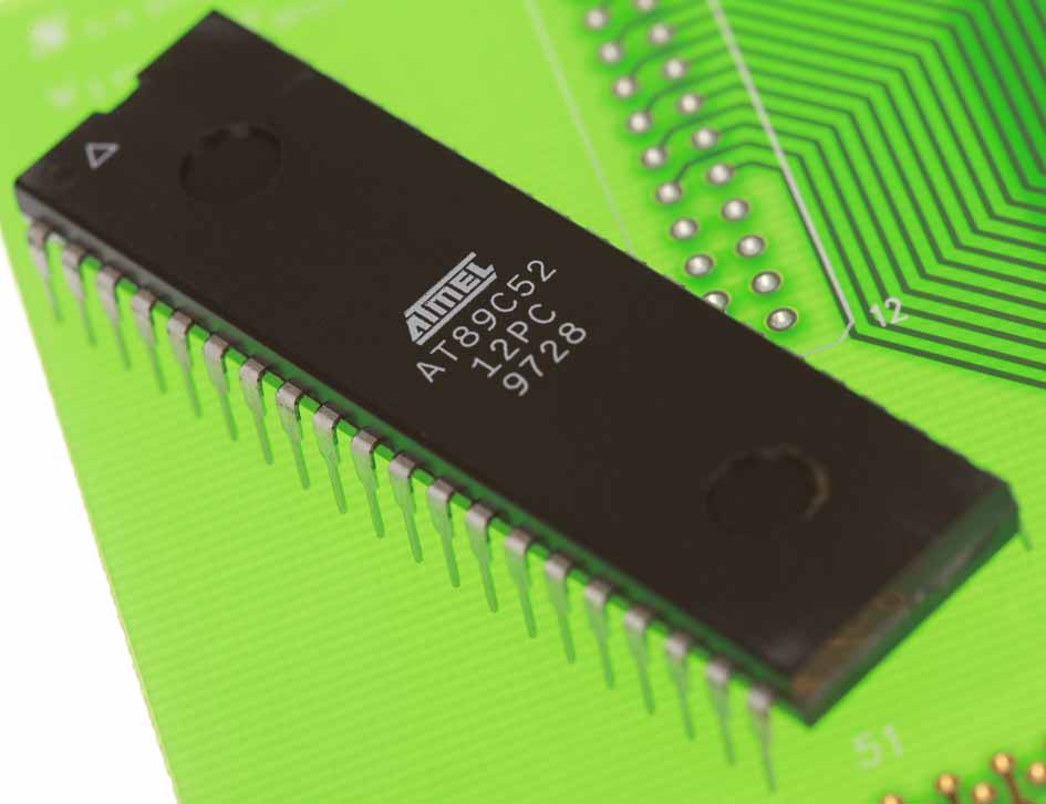
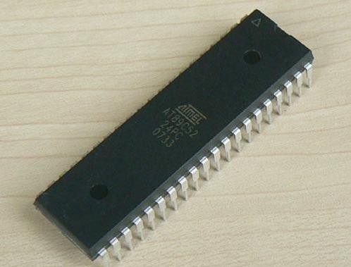
AT89C52 is an 8-bit microcontroller and belongs to Atmel’s 8051 family. AT89C52 has 8KB of Flash programmable and erasable read only memory (PEROM) and 256 bytes of RAM. AT89C52 has an endurance of 1000 Write/Erase cycles which means that it can be erased and programmed to a maximum of 1000 times.
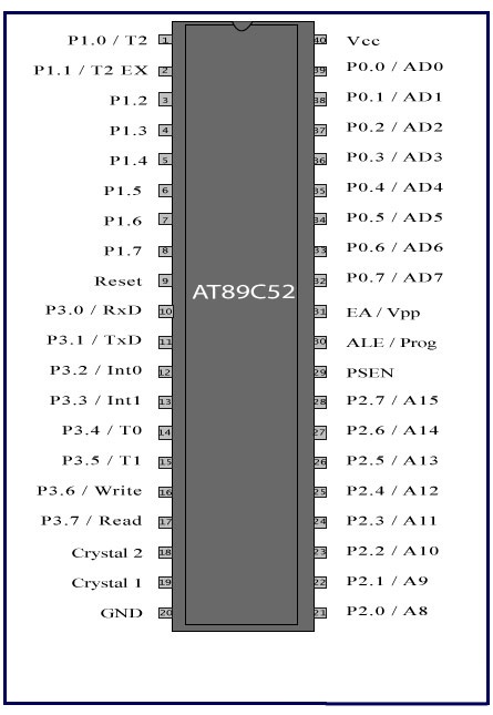
Though very slight difference between the features of AT89C51 and AT89C52, they are very similar in their pin configurations* and operations. Thedifferences between AT89C51 and AT89C52 have been tabulated below.
| AT89C52 | AT89C51 | |
| RAM | 256 Bytes | 128 Bytes |
| Flash | 8 KB | 4 KB |
| Number of Timers/Counters | 3 (16-bit each) | 2 (16-bit each) |
| Number of Interrupt Sources | 8 | 6 |
*The pin configuration of AT89C52 is exactly similar to that of AT89C51 except that the first two pins, P1.0 and P1.1 are multiplexed to correspond to Timer2 operations as given in the following table.
| Existing | Alternate | Function |
| P1.0 | T2 | Timer/counter 2 External Count input |
| P1.1 | T2 EX | Timer/counter 2 Trigger input |
While AT89C51 has two timers (Timer0 & Timer1), AT89C52 also has Timer2. Corresponding to Timer2, there are extra SFRs (Special Function Registers) T2CON & T2MOD. Also there are registers RCAP2H & RCAP2L to configure 16 bit Capture & Auto-reload modes of Timer2.
Pin Description:
| Pin No | Function | Name | |||
| 1 | External count input to Timer/Counter 2, clock-out | T2 | P1.0 | ||
| 2 | Timer/Counter 2 capture/reload trigger and direction control | T2 EX | P1.1 | ||
| 3 | 8 bit input/output port (P1) pins | P1.2 | |||
| 4 | P1.3 | ||||
| 5 | P1.4 | ||||
| 6 | P1.5 | ||||
| 7 | P1.6 | ||||
| 8 | P1.7 | ||||
| 9 | Reset pin; Active high | Reset | |||
| 10 | Input (receiver) for serial communication | RxD | 8 bit input/output port (P3) pins | P3.0 | |
| 11 | Output (transmitter) for serial communication | TxD | P3.1 | ||
| 12 | External interrupt 1 | Int0 | P3.2 | ||
| 13 | External interrupt 2 | Int1 | P3.3 | ||
| 14 | Timer1 external input | T0 | P3.4 | ||
| 15 | Timer2 external input | T1 | P3.5 | ||
| 16 | Write to external data memory | Write | P3.6 | ||
| 17 | Read from external data memory | Read | P3.7 | ||
| 18 | Quartz crystal oscillator (up to 24 MHz) | Crystal 2 | |||
| 19 | Crystal 1 | ||||
| 20 | Ground (0V) | Ground | |||
| 21 | 8 bit input/output port (P2) pins/
High-order address bits when interfacing with external memory
|
P2.0/ A8 | |||
| 22 | P2.1/ A9 | ||||
| 23 | P2.2/ A10 | ||||
| 24 | P2.3/ A11 | ||||
| 25 | P2.4/ A12 | ||||
| 26 | P2.5/ A13 | ||||
| 27 | P2.6/ A14 | ||||
| 28 | P2.7/ A15 | ||||
| 29 | Program store enable; Read from external program memory | PSEN | |||
| 30 | Address Latch Enable | ALE | |||
| Program pulse input during Flash programming | Prog | ||||
| 31 | External Access Enable; Vcc for internal program executions | EA | |||
| Programming enable voltage; 12V (during Flash programming) | Vpp | ||||
| 32 | 8 bit input/output port (P0) pins
Low-order address bits when interfacing with external memory
|
P0.7/ AD7 | |||
| 33 | P0.6/ AD6 | ||||
| 34 | P0.5/ AD5 | ||||
| 35 | P0.4/ AD4 | ||||
| 36 | P0.3/ AD3 | ||||
| 37 | P0.2/ AD2 | ||||
| 38 | P0.1/ AD1 | ||||
| 39 | P0.0/ AD0 | ||||
| 40 | Supply voltage; 5V (up to 6.6V) | Vcc | |||


