

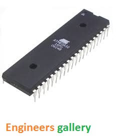
ATmega32 is very much similar to ATmega16 microcontroller with certain differences which are discussed below. ATmega32 is an 8-bit high performance microcontroller of Atmel’s Mega AVR family. Atmega32 is based on enhanced RISC (Reduced Instruction Set Computing) architecture with 131 powerful instructions. Most of the instructions execute in one machine cycle. Atmega32 can work on a maximum frequency of 16MHz.
The differences between ATmega32 and ATmega16 can be summarized as follows:
- ATmega32 has 32 KB programmable flash memory, static RAM of 2 KB and EEPROM of 1 KB. The endurance cycle of flash memory and EEPROM is 10,000 and 100,000, respectively.
| ATmega32 | ATmega16 | |
| RAM | 2 KB | 1 KB |
| Flash | 32 KB | 16 KB |
| EEPROM | 1 KB | 512 bytes |
- The Bootloader area, the NRWW section starts at word 0x3800 in ATmega32 while in ATmega16 it starts at 0x1C00.
- ATmega32 has a different interrupt table, the table given below shows the difference. More details can be obtained from the respective datasheets.
| Vector # | ATmega32 | ATmega16 |
| 1 | Reset | Reset |
| 2 | INT0 | INT0 |
| 3 | INT1 | INT1 |
| 4 | INT2 | Timer2 COMP |
| 5 | Timer2 COMP | Timer2 OVF |
| 6 | Timer2 OVF | Timer1 CAPT |
| 7 | Timer1 CAPT | Timer1 COMPA |
| 8 | Timer1 COMPA | Timer1 COMPB |
| 9 | Timer1 COMPB | Timer1 OVF |
| 10 | Timer1 OVF | Timer0 OVF |
| 11 | Timer0 COMP | SPI, STC |
| 12 | Timer0 OVF | USART, RXC |
| 13 | SPI, STC | USART, UDRE |
| 14 | USART, RXC | USART, TXC |
| 15 | USART, UDRE | ADC |
| 16 | USART, TXC | EE_RDY |
| 17 | ADC | ANA_COMP |
| 18 | EE_RDY | TWI |
| 19 | ANA_COMP | INT2 |
| 20 | TWI | Timer0 COMP |
| 21 | SPM_RDY | SPM_RDY |
- In MCUCR register, the SM2 and SE bits are swapped, i.e., the SM2 bit is bit7 and SE bit is bit6 in MCUCR register in ATmega32.
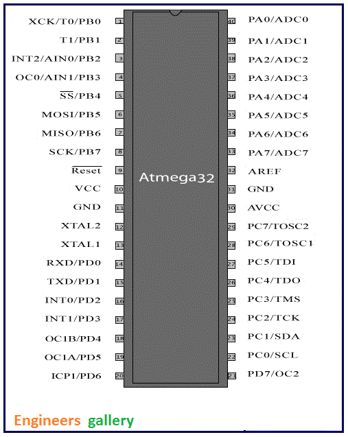
Pin Description:
| Pin No. | Pin name | Description | Alternate Function |
| 1 | (XCK/T0) PB0 | I/O PORTB, Pin 0 | T0: Timer0 External Counter Input.XCK : USART External Clock I/O |
| 2 | (T1) PB1 | I/O PORTB, Pin 1 | T1:Timer1 External Counter Input |
| 3 | (INT2/AIN0) PB2 | I/O PORTB, Pin 2 | AIN0: Analog Comparator Positive I/PINT2: External Interrupt 2 Input |
| 4 | (OC0/AIN1) PB3 | I/O PORTB, Pin 3 | AIN1: Analog Comparator Negative I/POC0 : Timer0 Output Compare Match Output |
| 5 | (SS) PB4 | I/O PORTB, Pin 4 | In System Programmer (ISP)Serial Peripheral Interface (SPI) |
| 6 | (MOSI) PB5 | I/O PORTB, Pin 5 | |
| 7 | (MISO) PB6 | I/O PORTB, Pin 6 | |
| 8 | (SCK) PB7 | I/O PORTB, Pin 7 | |
| 9 | RESET | Reset Pin, Active Low Reset | |
| 10 | Vcc | Vcc = +5V | |
| 11 | GND | GROUND | |
| 12 | XTAL2 | Output to Inverting Oscillator Amplifier | |
| 13 | XTAL1 | Input to Inverting Oscillator Amplifier | |
| 14 | (RXD) PD0 | I/O PORTD, Pin 0 | USART Serial Communication Interface |
| 15 | (TXD) PD1 | I/O PORTD, Pin 1 | |
| 16 | (INT0) PD2 | I/O PORTD, Pin 2 | External Interrupt INT0 |
| 17 | (INT1) PD3 | I/O PORTD, Pin 3 | External Interrupt INT1 |
| 18 | (OC1B) PD4 | I/O PORTD, Pin 4 | PWM Channel Outputs |
| 19 | (OC1A) PD5 | I/O PORTD, Pin 5 | |
| 20 | (ICP) PD6 | I/O PORTD, Pin 6 | Timer/Counter1 Input Capture Pin |
| 21 | PD7 (OC2) | I/O PORTD, Pin 7 | Timer/Counter2 Output Compare Match Output |
| 22 | PC0 (SCL) | I/O PORTC, Pin 0 | TWI Interface |
| 23 | PC1 (SDA) | I/O PORTC, Pin 1 | |
| 24 | PC2 (TCK) | I/O PORTC, Pin 2 | JTAG Interface |
| 25 | PC3 (TMS) | I/O PORTC, Pin 3 | |
| 26 | PC4 (TDO) | I/O PORTC, Pin 4 | |
| 27 | PC5 (TDI) | I/O PORTC, Pin 5 | |
| 28 | PC6 (TOSC1) | I/O PORTC, Pin 6 | Timer Oscillator Pin 1 |
| 29 | PC7 (TOSC2) | I/O PORTC, Pin 7 | Timer Oscillator Pin 2 |
| 30 | AVcc | Voltage Supply = Vcc for ADC | |
| 31 | GND | GROUND | |
| 32 | AREF | Analog Reference Pin for ADC | |
| 33 | PA7 (ADC7) | I/O PORTA, Pin 7 | ADC Channel 7 |
| 34 | PA6 (ADC6) | I/O PORTA, Pin 6 | ADC Channel 6 |
| 35 | PA5 (ADC5) | I/O PORTA, Pin 5 | ADC Channel 5 |
| 36 | PA4 (ADC4) | I/O PORTA, Pin 4 | ADC Channel 4 |
| 37 | PA3 (ADC3) | I/O PORTA, Pin 3 | ADC Channel 3 |
| 38 | PA2 (ADC2) | I/O PORTA, Pin 2 | ADC Channel 2 |
| 39 | PA1 (ADC1) | I/O PORTA, Pin 1 | ADC Channel 1 |
| 40 | PA0 (ADC0) | I/O PORTA, Pin 0 | ADC Channel 0 |


