

Introduction:
This project illustrates the use of a V/F converter in monitoring temperature in degrees Fahrenheit (0F). The block diagram of the temperature indicator is shown in Figure 1-1. The indicator is composed of a temperature sensor, amplifier, V/F converter, three-digit binary-coded-decimal (BCD) counter, time base, and LED display In addition to the 9400 V/F converter, other ICs needed for this project include the LM334 temperature sensor, LF353 dual op-amp, NE555 timers, 74LS00 NAND gate, MC14553 three-digit BCD counter. MC14543 BCD-to-seven segment decoder/driver/latch and three seven-segment (common anode or common cathode) LED displays with three PNP switching transistors.

Working of the system:
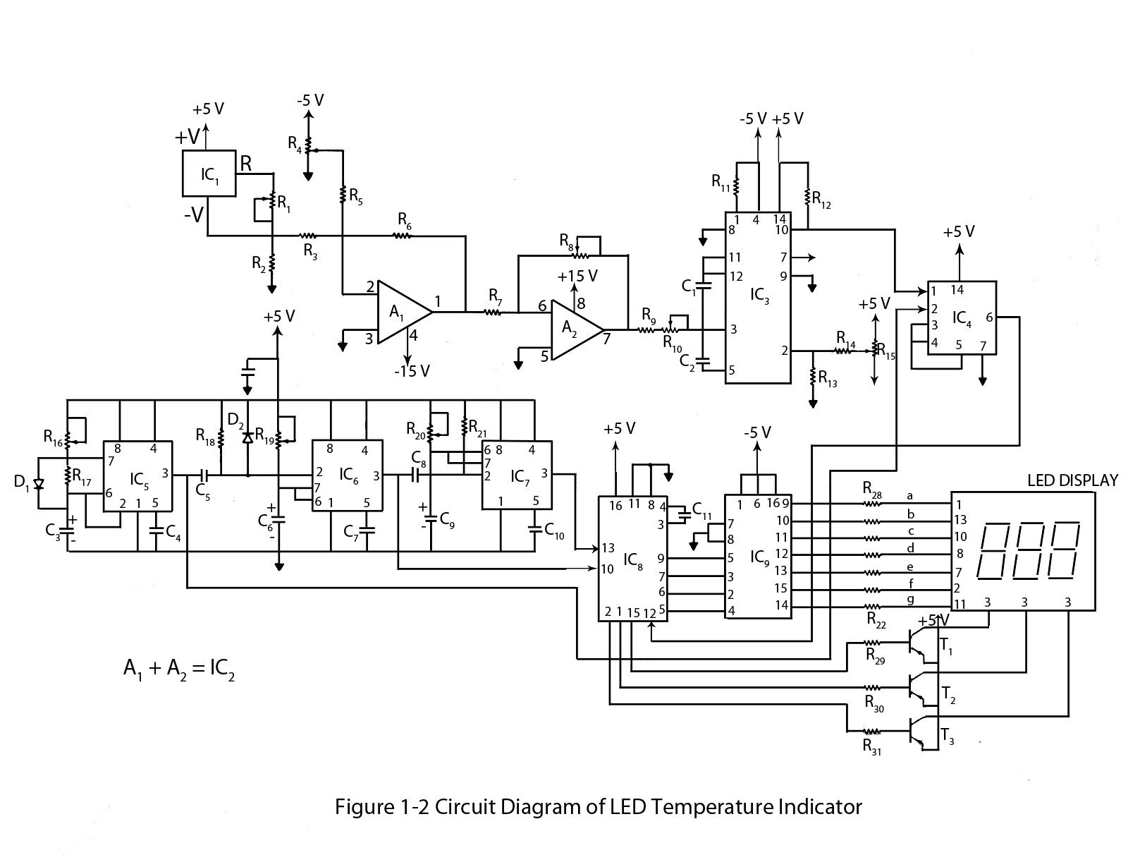
Figure 1-1 shows the schematic diagram, which is designed to display temperatures from 0° to 100°F. Operation of the circuit is as follows. The output of the temperature sensor changes linearly as a function of temperature (10 mV/ K). This output is an input to the summing amplifier, which is used to calibrate the output of the temperature sensor for a desired temperature type (K, 0C, or 0F) and an intended range. That is, to display the temperature in either K, °C, or 0F, potentiometer R4 is adjusted accordingly so that a suitable voltage appears at the output of the summing amplifier. Since the output of the temperature sensor is directly proportional to temperature changes-, R4 needs to be adjusted at only one temperature. The output of the summing amplifier then drives the inverting amplifier. The purpose of the inverting amplifier is twofold: (1) to invert the input so that its output voltage is positive, which is necessary for the V/F converter, and (2) to provide a suitable gain, which depends on the voltage-to-frequency scaling used for the V/F converter.
The output of the inverting amplifier is the input to the V/F converter; therefore, the output frequency of the converter is directly proportional the output voltage of the inverting amplifier. For example, as the temperature goes up the output voltage of the summing amplifier increases in the negative direction, Whereas that of the inverting amplifier increases in the positive direction, which in turn causes the frequency of the V/F to increase in the positive direction.
The output frequency of the converter is then ANDed with the gating signal to produce the clock signal for the three-digit BCD counter. The BCD output of the counter drives the three LED displays sequentially via the BCD-to-seven segment decoder/latch/driver stage, and the temperature is displayed on the LEDs, depending on the relationship between the frequency of the V/F converter and the gate signal. The gate, latch, and reset signals are generated by the time-base circuit, which consists of a free-running multivibrator and two one-shot multivibrators.
PARTS LISTS
Resistors (all ¼-watt, ± 5% Carbon)
- R1 = 1 kΩ potentiometer at 230 Ω
- R2, R7, R12, R13, R21 = 10 kΩ
- R3, R5, R6, R11 = 100 kΩ
- R4 = 10 kΩ potentiometer
- R8= 1 MΩ potentiometer
- R9 = 180 kΩ
- R10, R15 = 50 kΩ potentiometer
- R14 = 510 kΩ
- R16 = 3 kΩ potentiometer
- R17 = 15 kΩ
- R18 = 20 kΩ
- R19 = 10 kΩ potentiometer
- R20 = 1 kΩ potentiometer
- R22 – R28 = 220 Ω
- R29 – R31 = 1k Ω
Capacitors
- C1 = 1000 pF
- C2 = 100 pF
- C3, C6, C9 = 1 µF
- C4, C5, C7, C8, C10 = 0.01 µF
- C11 = 0.001 µF
Semiconductors
- IC1 = LM334 temperature sensor
- IC2 = LF353 dual op-amp
- IC3 = Teledyne 9400 V/F convertor
- IC4 = 74LS00 NAND gate
- IC5, IC6, IC7 = NE/SE 555 timers
- IC8 = MC 14553 three-digit BCD counter
- IC9 = MC 14543 BCD-to-seven segment decoder/driver/latch
- Q1, Q2, Q3 = 2N1305 switching transistors
- D1, D2 = 1N914 signal diodes
- Three seven-segment common anode LEDs: MAN72A or equivalent
Circuit Description
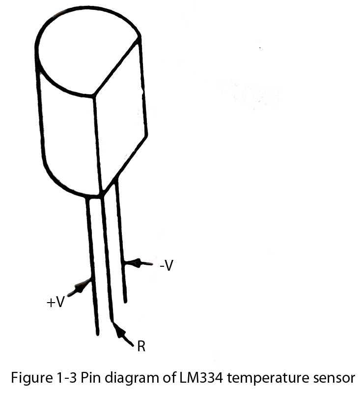
Next let us examine the design considerations and procedures for each of the sections in the temperature indicator of Figure l-2. The temperature sensor LM334 is a three-terminal adjustable current source whose current can be programmed from 1µ to 10 mA with one external resistor R1. The three terminals are labeled +V, R, and –V. The pin diagram of the LM334 is shown separately in Figure 1-3.
The LM334 has a wide operating voltage range of 1 to 40 V. It can also withstand reverse voltage of up to 20 V(terminal + V is negative with respect to –V). It is designed to operate over a temperature range of 0° to 70°C. For a wider temperature range, such as -550 to 150°C, Intersil’s AD590 temperature sensor is recommended.
For the values indicated in Figure 1-2, the output of the LM334 changes 10 mV/K. This means that at 00F = 255.22 K the output of the sensor will be 2552.2 mV, which must be scaled down to 0 V so that the temperature displayed will be in degrees Fahrenheit. This is accomplished by the use of the summing amplifier. Specifically, potentiometer R4 of the summing amplifier is adjusted so that the output is 0 V. The same procedure is used to calibrate the output of the summing amplifier at any other value of 0F. Table 1-1 shows the relationship between K, °C, 0F, and the output of the temperature sensor and the summing amplifier at corresponding values of temperature. Because the output of the sensor directly proportional to the temperature, the output of the summing amplifier needs to be calibrated at the temperature at which the circuit is initially started up (refer to Table 1-1).
Table 1-1 RELATIONSHIP BETWEEN DIFFERENT TEMPERATURE UNITS AND OUTPUTS OF THE SENSOR AND SUMMING AMPLIFIER
| Kelvin (K) | Degrees Celsius | Degrees Fahrenheit | Output of the temperature sensor (mV) | Output of the summing amplifier (mV) to be adjusted to |
| 255.22 | -17.78 | 0 | 2552.2 | 0 |
| 273 | 0 | 32 | 2730 | -177.8 |
| 298 | 25 | 77 | 2980 | -427.8 |
| 310.78 | 37.78 | 100 | 3107.8 | -555.6 |
Note that the output of the summing amplifier is a negative dc voltage since the net input voltage is always positive for temperatures >00 (see Table 1-1). However, the 9400 V/F requires a positive input voltage. The summing amplifier must be therefore be followed by an inverting amplifier. The gain of the inverting amplifier, however, depends on the voltage-to-frequency scaling of the convertor. The V/F convertor of figure 1-2 is calibrated for the maximum frequency of 50 KHz, which represents a temperature of 1000F when the input voltage is 10 V maximum. Since the output of the summing amplifier is -555.6 mV at 1000F, the gain of the inverting amplifier must be equal to
10V/555.6mV = 17.9985
The output frequency of the V/F converter is then ANDed with the output frequency (called the gate signal) of the 555 free-running multivibrator to produce the clock signal for the three-digit BCD counter. Since the maximum 50-kHz output frequency of the converter represents 1000F, the three-digit BCD counter must be clocked 100 times to display I00°F. To accomplish this, the pulse width of the free-running multivibrator must be 100/50 K = 2 ms so that 100 pulses will be produced in 2 ms. At the end of 2 ms, the count of the counter is latched and displayed on the LED display. After the count is displayed as a temperature on the LEDs, the BCD counter is reset and the cycle repeats. In other words, the counter continuously cycles through three states: count, latch, and reset. Therefore, the free-running multivibrator (gate signal) must provide for the time period required to count, latch, and reset the BCD counter. The latch enable and master reset pulses for the BCD counter MCl4553 are produced by using two 555 one-shot multivibrators. Where the time period of the free-running multivibrator is approximately 12.5 ms with a pulse width of 2 ms. The pulse width of the latch enable pulse is approximately 10 ms, and the master reset pulse width is approximately 0.5 ms. To accomplish 2-, 10-, and 0.5-ms pulse widths, adjust potentiometers R16, R18, and R20, respectively (Figure l-2).
The three-digit BCD counter used in Figure 1-2 is the MC14553. The MCl4553 consists of three negative-edge-triggered BCD counters with a quad latch at the output of each counter, which enables the storage of any given count. The outputs of the latches are time multiplexed so that one BCD digit at a time is produced. The operation of the multiplexer output selector is controlled by the on-chip oscillator, whose frequency depends on the external capacitor.
As shown in Figure 1-2, the master reset (MR) and latch enable (LE) pulses for the MC14553 are produced by using two 555 one-shot multivibrators. In addition, the clock signal for the MC14553 is produced by ANDing the output of the V/F converter with the gating signal, which is obtained by using the 555 free-running multivibrator. The digit select outputs DS1, DS2, and DS3 sequentially drive the 2N1305 PNP transistors T1, T2, and T3, which in turn control the three LED displays. The BCD outputs of the MCl4553 are connected to the BCD inputs of the MCl4543, which is a BCD-to-seven segment latch/decoder/driver. The seven-segment outputs of the MCl4543 then drive the seven segments of the LED selected by the digit-select of the MC14553.
The MCl4543 is designed to provide three functions: a 4-bit storage latch, an 8421 BCD-to-seven segment decoder, and a driver. The device is capable of driving LCD and LED displays.
The PH pin 6 of the MC14543 is connected to VDD (logic 1) because the LED displays are the common anode type. To limit the current through each of the LED segments, a separate resistor is used in series with each segment. Note, however, that only seven resistor are required for all the segment of LEDs. This is possible because the digit-select output of the MC14553 function sequentially. In addition, the BCD output are also multiplexed, one BCD digit at a time.
Finally, since the accuracy of the temperature displayed depends mainly on the frequency stability of the free-running multivibrator, all resistors must be of 5% or better tolerance, and capacitor must be either Mylar of tantalum types.
Also remember that the temperature indicator must be calibrated at a temperature at which it is initially turned on.


